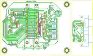
Errors at the beginning of the product development cycle are the most expensive errors of all. Thus, to guarantee a functional circuit design, the DRC will validate the Gerber data, and identify the potential design errors before the manufacturing process.
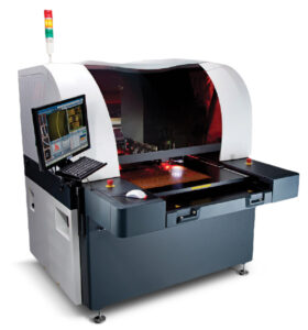
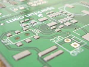
AOI is an automated visual inspection of a PCB’s inner and outer layers. A camera autonomously scans the layer under test for both catastrophic failure (e.g. missing features such as pads, holes, etc.) as well as quality defects (e.g. Line width and spacing, short and open circuits, cuts, excess copper, etc.). Since this inspection is much more reliable and repeatable than the manual visual check, 100% of the PCBs go through an AOI.

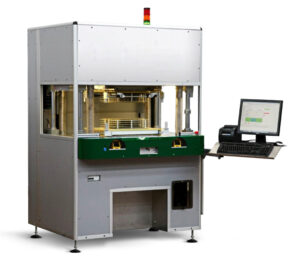
Whether a “Flying Probe” or “Bed of Nails” is used, the outcome of the E-test will ensure that all the boards are Short and Open Circuit free. Regardless of the batch size, we guarantee that 100% of the PCBs undergo this Electric Check.
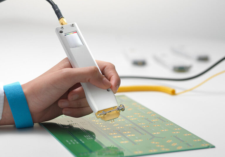
For a small volume of PCBs, a test program is used to electro-mechanically control a set of probes. These probes perform a full Continuity and Isolation inspection of the interconnects and conductive nodes on the circuit board.
For a medium to large volume of PCBs, a jig containing a bed of nails is built specifically for each circuit board. As its name suggests, this jig contains numerous probes that are aligned to make contact with all the test points on the PCB. Within a split of a second, the full board is tested for Open and Short circuits.
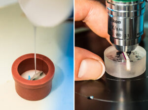
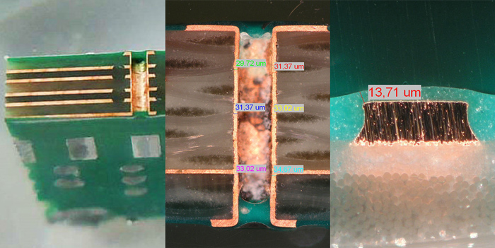
The Micro-Section is a destructive test in which a small section is taken out of a circuit board sample and encapsulated in a transparent medium. The enclosed PCB slice is then analyzed by placing it behind the light of a Digital Microscope. Below is a list of some of the evaluated characteristics:
• Cross-Sectional dimensions
• Inner structure integrity (for multilayer boards)
• Laminate defects (Voids, cracks etc.)
• Copper layer thickness
• Copper thickness on plated through-holes
• Soldermask thickness
• Surface finish thickness
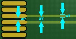
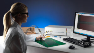
The impedance of a trace is a critical aspect for a functioning PCB. On some high speed communication boards, traces should have a tolerance of less than 5%. For this reason, a Network Analyzer or Time Domain Reflectometer (TDR) is used to measure these values.
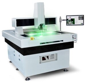
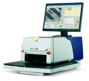
A “CNC Vison Measuring System” is used to run a full dimensional scan on the PCB. This will guarantee that the circuit board is accurately manufactured according to the Gerber data and will ensure that all the values are within the requested tolerances.
A Micro-Section is a destructive test that evaluates the copper thickness of one PCB.
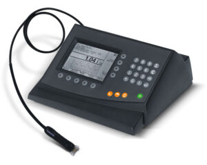
In order to assess this thickness for all the produced boards, a “Thru-Hole” & “Copper Surface Gauge” is used to non-destructively measure the deposited copper value.
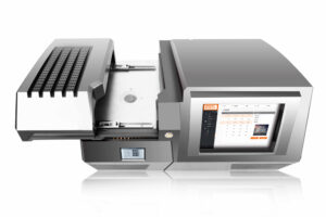
The PCB surface finish has two essential functions, to protect the exposed copper circuitry and to provide a solderable surface when assembling the components. To make sure that the boards are properly coated, an “X-Ray Fluorescence-XRF” is used to analyze the PCB thin coatings (e.g. Au, Ag, Pd, Sn, etc.).
An “RoHS XRF Tester” examines the PCB composition content and guarantees that the six hazardous materials (Pb, Hg, Cd, Cr6+, PBB, PBDE) are within the allowable limits.

Ionic contamination can cause a variety of defects, including corrosion, degradation, metallization and rapid deterioration of wire bond interconnects. For this reason, “Ionic Contamination Testers” are used to confirm that the PCBs meet the IPC Cleanliness requirements.
The Solderability test evaluates the strength and wetting quality of a solder. The solder paste is applied on the empty PCB to simulate the latter’s behavior when mounting the components on the board.
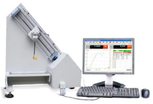
To assess the bonding strength between the copper and the laminate, a “Peel Strength Tester” is used to measure the required force that will shear a copper trace from the board.
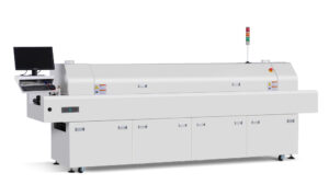
The Thermal Stress test is designed to determine the integrity of a PCB by exposing it to a certain high temperature. This inspection can also be done in an “IR Reflow” oven by subjecting the board to same temperature profile used in the component assembly process.
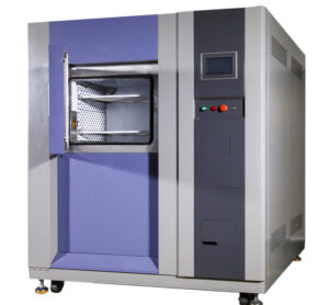
In a “Climate Control Room”, mechanical stresses are induced on a PCB by subjecting it to alternating high and low temperature extremes. The Thermal Shock test determines the board’s physical endurance by analyzing the implications caused by these sudden changes in temperature.